Nanopatterning
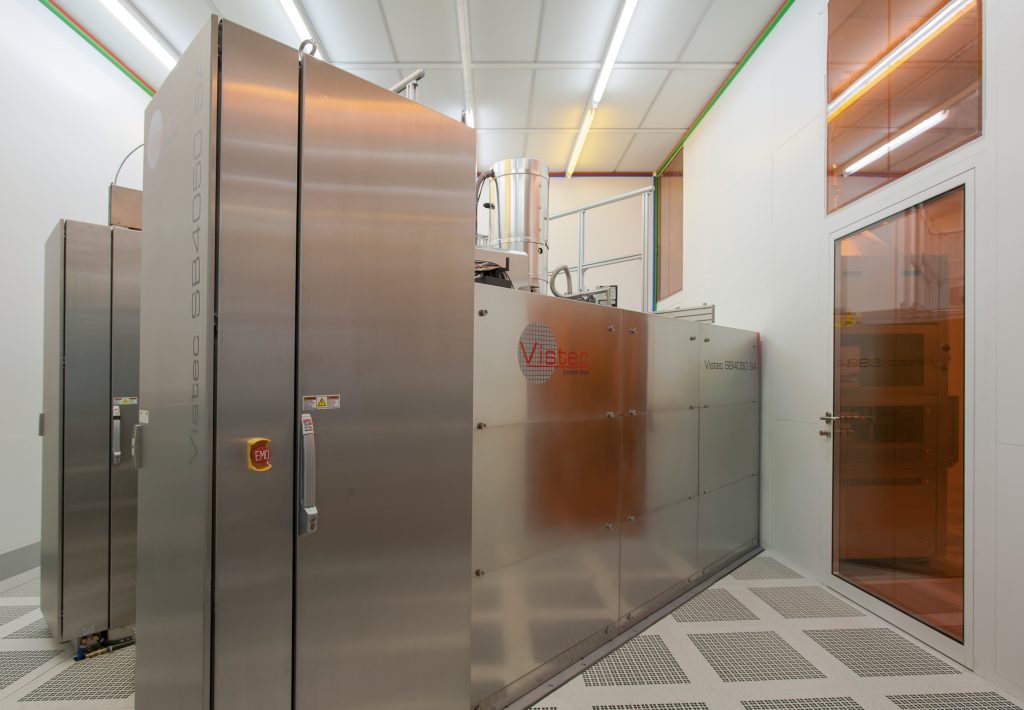
IMS CHIPS looks back on more than 30 years of experience in the field of electron beam lithography for the production of high-resolution, complex structures. We are currently working with the third generation equipment, consisting of two shape beam writers from Vistec for substrate sizes between 150 mm and 450 mm. Using the appropriate equipment, as an example of our range of products, we manufacture nano-imprint masters, optical elements and masks for the highest demands at an industrial level.
To complement electron beam lithography, we operate two laser direct write systems (resolution up to 0.7um) and an I-line stepper (resolution up to 0.4um). These are also mix-and-match compatible with our electron beam writers and thus allow a cost-efficient implementation of patterns with different resolution requirements.
We´ll gladly evaluate the implementation of special customer requirements or develop processes tailored to the respective application. Contact us!
Our idea - our mission
In close cooperation with our customers, we develop technologies, processes and components. The developed products can be qualified in our technology department and, if desired, manufactured as a single product or certified in a small series.
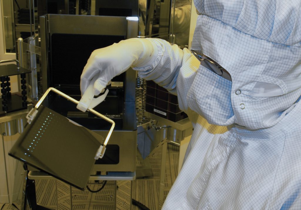
In cooperation with equipment and material manufacturers, we evaluate their products in our line so that they can be demonstrated to potential customers. For example, our partner Heidelberg Instruments uses the IMS clean room to demonstrate the ULTRA laser writer.
Contact
Julian Hartbaum
email: Julian Hartbaum

In close cooperation with our customers, we develop technologies, processes and components. The developed products can be qualified in our technology department.
In cooperation with equipment and material manufacturers, we evaluate their products in our line so that they can be demonstrated to potential customers. For example, our partner AP&S uses the IMS clean room to demonstrate the “Multistep” cleaner.
The IMS offers position measurements on the LMS-IPRO as one of our many services to you.
Product samples
Nano-Imprint Templates
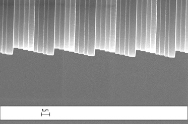
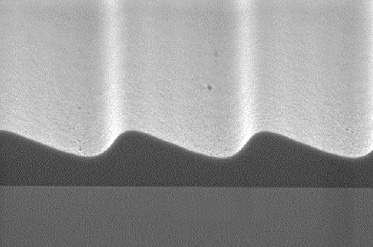
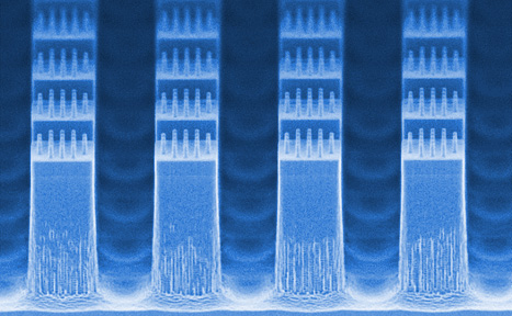
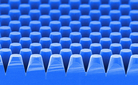
We manufacture replication masters based on silicon wafers, quartz wafers, mask blanks or SOI wafers. RIE and ICP processes, as well as Bosch and cryo-etching processes are available as structure transfer technologies. Subsequent surface treatments allow the masters to be professionally cleaned, smoothed and provided with a non-stick coating.
Wafers can be separated on request. Form factors thus range from a few mm² to 230 x 230 mm².
In addition to binary structures, multi-level, mesa structures and, in photo resist, 3D analog structures can be realized.
Optical Elements
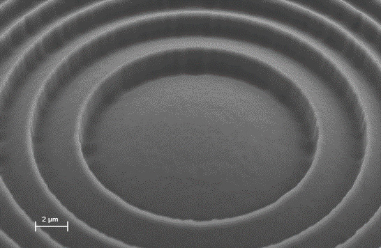
Many customers with optical applications take advantage of our ability to precisely pattern complex structures in quartz glass even in the sub-micrometer range.
150 mm or 200 mm quartz wafers or square mask substrates in sizes 6” (6025) and 9” (9035) serve as a basis. Lines for round 12” or 17” substrates are available for special applications.
Typical applications are Fresnel lenses, microlens arrays or diffractive optical elements.
Masks
MS has been operating its own mask line for over 15 years. The equipment allows the processing of binary as well as phase-shifted masks in the 6025 and 9035 formats. On the one hand, we offer a solution from a single source to our customers, however, we also use the processes for other applications based on masks
Resist technology
For an electron lithographic implementation of high-resolution and complex structures at an acceptable throughput, we are continuously evaluating resists for e-beam applications together with our suppliers and potential users and are developing processes with selected samples.
The resists are evaluated for their performance parameters, such as resolution, stability, and sensitivity, and the processes are tailored to the specific application.
To eliminate charging effects during the e-beam exposure, combinations of resists with conductive layers have been successfully implemented.
