Completed projects
 |
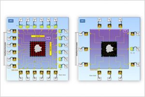
NeMoH – Microelectronics for AI – Neuromorphic HardwareIn the project “Microelectronics for AI – Neuromorphic Hardware”, supported by the state of Baden-Württemberg, three industry-related research institutes of the Baden-Württemberg Innovation Alliance are researching and developing adaptive, safe and energy-efficient AI chips. These are considered as an elementary prerequisite for applications in the field of Industrie 4.0 and the Internet of Things (IoT). The project is coordinated by the Institut für Mikroelektronik Stuttgart (IMS CHIPS). Together with the Forschungszentrum Informatik (FZI), and the Hahn-Schickard-Gesellschaft für angewandte Forschung e. V. accompanied by an industry advisory board the project has started in mid-2019. Project duration: June 25th, 2019 thru December 31st, 2020 For further information the “Mikroelektronik für KI – Neuromorphe Hardware” research project, please refer to: NeMoH |
 |
MULTI-3D – focus-modulating 3D sensor systemAs part of the sponsoring program “Photonik Forschung Deutschland” the research project MULTI-3D will be developing a micro-optical 3D sensor system to determine and/or measure 3D objects. The “High-dynamic linear CMOS image sensor” project part will have Institut für Mikroelektronik Stuttgart developing an image sensor that is able to acquire a very high dynamic range. Just like many other image acquisition processes the anticipated micro-optical 3D sensor system will be able to record a very high luminance range of the detected objects as well as an interfering light of the surrounding conditions. Project duration: February 1st, 2017 thru December 31st, 2020 |
 |
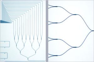
Fiber Coupling – Photonic interconnection technology with optimized coupling efficiencyThe signal technical connection of photonic components is made using optical fibers, which couple light into the chips via microscopic structures (grid couplers). The efficiency of this fiber coupling is decisive for the overall properties of the circuit. Currently there is a conflict of objectives between the necessary coupling efficiency and throughput capability of the relevant procedures (glass fibers need to be precisely aligned and attached in six axes). The project´s objective is to develop new grid couplers with a particularly high degree of couple efficiency which simultaneously meet future cost requirements using processes and procedures suitable for mass production. The main idea is to create guide structures in the form of buried structures in the wafer using special laser-assisted etching processes, into which the fibers are inserted. IMS CHIPS will be developing an etching process which removes the laser-treated structures in silicon with higher selectivity than the untreated structures. The developmental work within the scope of the project include individual processing steps in a known production process. Project duration: November 1st, 2018 thru October 31st, 2020 |
 |
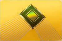
HDRC-AeroPantoCamThe 2-year ZIM project was launched in July 2018. Project partners are KST GmbH – Kamera & System Technik and GEVITEC. Project duration: July 1st, 2018 thru June 30th, 2020 |
 |
FLEXMAX – flexible active sensor matrix for medical applicationsThe BMBF sponsored project “FLEXMAX” was launched April 1st, 2018. Project duration: April 1st, 2018 thru June 31st, 2021 For further information on the FLEXMAX research project, please refer to: www.elektronikforschung.de/projekte/flexmax |
 |
BW-CPS – smart intelligent energy-efficient sensor systemsThe new “BW-CPS” project (CPS = cyber-physical systems) is an initiative sponsored by the Baden-Württemberg government for the development of a modular system component kit for intelligent and energy-efficient sensor systems for Industrie 4.0. By showing 4 practical cases of application the potential of the system component kit for future production facilities is demonstrated. This is about monitoring energy flow, controlling air conditioning, collecting processing data in in-molds as well as optimizing intralogistics and navigational components. All of this is done in close cooperation with the industrial sector which benefits from all of the newly developed functions that are thus becoming available. Apart from IMS CHIPS the FZI and Hahn-Schickard are participating in the BW-CPS project. Project duration: April 7th, 2017 thru February 29th, 2020 |
 |
GaNScan – mapping and modeling of GaN/Si wafers for power electronic applicationsAs part of the KMU-innovativ project GaNScan transistors and testing structures made of the compound semicondutor gallium nitride (GaN) are to be produced and researched on silicon wafers with epitaxy layers. These structured are used for space-resolved measurement (mapping) of testing and component parameters. This is done to research new structures and increase the measurement and test engineering competences in order to extract key parameters. The extracted parameters will offer an inside into the quality and characteristics of the substrate and epitaxy. This crucial information is returned to the epitaxial distributor to improve the reliability and quality of the transistors. Project partners are RoodMicrotech (projekt management, KMU), AdMOS (KMU) and IMS CHIPS. Project timetable: September 1st, 2017 thru February 29th, 2020 |
 |
C-GaN – Complementary GaN Transistors for Logic Devices in High-temperatureThe scope of the “C-GaN” project in cooperation with RWTH Aachen University (Compound Semiconductor Technology, Lehrstuhl für Höchstfrequenzelektronik) is to explore the technical and physical limits of complementary gallium nitride (GaN) transistors for logic devices in high-temperature (temperatures up to 1000 °C) and high-frequency applications. High-temperature applications, such as aerospace components, automotive electronics and oil drilling equipment, exceed temperature limits know in conventional silicon technology. Logic devices based on GaN can be implemented in high-temperature and high-frequency applications due to the outstanding material properties of GaN. In order to reach this goal a heterogeneous academic consortium has formed bringing together leading scientific groups in the field of nitride materials and device technology, high-temperature characterization and packaging technology, and also, RF testing, modelling and circuit design. Project timetable: May 1st, 2017 thru January 31st, 2020 |
 |
Energy filter – Development of large-scale energy filter membrane for single wafer ion implant in silicon carbideIn a ZIM-promoted project the IMS and the new start-up mi2-factory are joining together for technological processes on the high-energy ion implantation of SiC power semiconductors. The focus, however, is on the Stuttgart-based development of large-scale and high-precision Si membrane masks, so-called energy filter membranes. Project timetable: April 1st, 2017 thru March 29th, 2019 |
 |
TAKEMI5 – technology Advances and Key Enablers for Module Integration for 5 nmIn line with industry needs, Moore’s law, scaling in ITRS 2013/2015, and ECSEL JU MASP 2016, the main objective of the TAKEMI5 project is to discover, develop and demonstrate lithographic, metrology, process and integration technologies enabling module integration for the 5 nm node. Project timetable:: April 1st, 2017 thru June 29th, 2019 |
 |
µHTS-CAN – micro High Troughput Screening Cell Adhesion Noise-(Spectroscopy)The KMU-Innovativ project µHTS-CAN is to develop a CMOS microchip-based imaging system for a speedy analysis of biological cells. This project is part of the Biotechnologie-BioChance sponsorship activities. This sub-project in which Institut für Mikroelektronik Stuttgart cooperates develops and tests processes to reliably create micro-structured surface structures from permanent photo resists (dry film resist) with integrated reference electrodes on Si chips. Project timetable: February 1st, 2017 thru July 31st, 2019 |
 |
innBW implant – Chip-in-foil systems for bio-electronic medicineBio-electronic micro implants are increasingly receiving more attention in the medical field. The tiny midgets can stimulate the neural system and, thus, be effectively used in the treatment of pain, migraine and depression as well as diabetes or high blood pressure. As of now, however, this development is still in its early stages. The research partnership combining of four Innovationsallianz Baden-Württemberg (innBW) research facilities is going to change this now. This research project is known as “innBW implant” and was launched on July 1st, 2015. The Ministry for Finance and Economy in Baden-Württemberg will be funding it with 3.65 mio. Euros. Project timetable: July 1st, 2015 thru December 31st, 2018 |
 |
NEMEZU – new precious metal-free membrane electrode units for future fuel cellsThe NEMEZU project will be researching and developing new precious metal-free membrane electrode units for alkaline fuel cells of the future. With a laser ablation on specially-selected precious metal-free materials and alloys the mass-implemented and cost-effective manufacture of catalytic layers for the use of micro-fuel cells will be developed. The effectiveness of alkaline fuel cells will be determined and measured during operation using infrared thermography of electro-chemical reactions. Project timetable: December 1st, 2015 thru November 31st, 2018 |
 |
ParsiFAl 4.0 – Product-capable autonomous and safe foil systems for automation solutions in Industrie 4.0IMS CHIPS has joint partners in the ParsiFAl 4.0 research project on the development of new sensors and electronics on thin foil. The ParsiFAl 4.0 research project which is supported by the Bundesministerium für Bildung und Forschung comprises several partners supported by the project administrator VDI/VDE-IT on the development of thin electronics systems, i e. Smart Sensor System (S3) labels. The foundation for S3 labels is micro controllers, sensors, thin displays and integrated communication interfaces, all of which are embedded into foils. The ascertained data can determine a component´s condition and, therefore, maintain equipment pro-actively. This reduces maintenance fees on production equipment significantly. Thus, transportation of critical goods can be tracked safely in the logistic and packaging field. Project timetable: November 1st, 2015 thru October 30th, 2018 Press release: ParsiFAl 4.0 |
SeNaTe – Seven Nanometer TechnologySeNaTe consists of 6 work packages focusing on lithography, metrology, processing, EUV mask infrastructure and a 7 nm process demonstration with one work package being reserved for project management. Project timetable: April 1st, 2015 thru March 31st, 2018 |
 |
MEMS-DMFC – Direct methanol fuel cell based on micro electric mechanical systemsThe ever increasing appetite for energy in portable electronics poses a particular challenge nowadays. Because of its enormous energy storage density a methanol-based fuel cell could just be the ideal solution opposed to traditional battery technologies. This AIF (Allianz Industrieforschung) sponsored project is set to run for 2.5 years and will be a cooperation with Zentrum für BrennstoffzellenTechnik ZBT GmbH. Project timetable: July 1st, 2015 thru December 31st, 2017 |
 |
SITARA – Self-adapting intelligent multi aperture camera modulesThe aim of the project is the development of cost-effective, intelligent and powerful cameras with a high-dynamic range as well as ashort face-to-face dimension of less than 3 mm. These outstanding properties are to be realized by developing synchronized high-dynamic range image sensors and special micro-optical systems.. Using micro and nano structuring technology, the optical components developed as demonstrators will be comparable to the naturally occurring compound eye. Course of the project: May 1st, 2014 thru September 30th, 2017 |
 |
Color Eye – high-dynamic color image sensor with new color and corrective algorithmsThe SME company hema electronic GmbH and IMS CHIPS are cooperating on the “ColorEye” project in developing particularly small new intelligent high-resolution video cameras based on the new HDRC® image sensor with Global Shutter technology. These cameras will be ideal for dynamic process control in sophisticated industrial applications, such as automation and assistance systems in hauling vehicles. Project timetable: September 1st, 2015 thru August 31st, 2017 |
 |
KATMETHAN – Catalytic methane synthesisThe target is to research new peptide-based catalysts for a methane synthesis as well as an increased and improved understanding of the complex conversion processes. The KATMETHAN project has an overall volume of 1.462 million € and is sponsored by the BMBF using 995,000 € in funds from the energy and climate fonds. IMS CHIPS is sponsored with 203,000 €. The project´s duration is three years. The project management agency is Projektträger Jülich, Geschäftsbereich Energietechnologie, Fachbereich Grundlagenforschung Energie (support code: 03EK3030D). Project timetable: September 1st, 2014 thru August 31st, 2017 |
 |
Smart-LiB – Intelligent Li ion batteries in production and useThe Smart-LiB project, a joint project between IMS CHIPS and the Innovationsallianz Baden-Württemberg (innbw) partner ZSW, was launched on October 1st, 2015, and is set to last until September 30th, 2016. This project is designed to research solutions to encompass the Li ion battery staple´s condition without the currently required wiring (SoH – State of Health, SoC – State of Charge). Project timetable: October 1st, 2015 thru March 31st, 2017 |
 |
TENECOR – Telemetric multimodal neonatal cortexmonitoringThe aim of this sub-project is the micro-electronic integration of a subsystem for safe automatic detection of EEG signals in preterm infants using a “electrode Cap”. The subsystem can be achieved as ASIC in addition to other components for the safe operation, error detection and data and status transmission to parent system parts of signal amplification, conditioning, and digitalisation. The subproject is an integral part of the demonstrator in the joint project designed with its fully integrated EEG – and impedance measuring circuit. Project timetable: March 1st, 2014 thru February 28tht, 2017 |
 |
KoSiF – Complex systems in foilThe KoSiF (Komplexe Systeme in Folie) research project researchs, evaluates and technologically adjusts the necessary technologies for additional functionalities that will be required for the manufacture of future thin and flexible products. KoSiF represents an initiative made up of industry, research facilities and universities aiming to find means of integration of thin silicon chips, thin-film components and organic electronics on one foil substrate enabling autonomous and intelligent flexible electronics. The project will realize two demonstrator, i. e. Smart Skin and Smart Switch, which will be connected to similar key technologies. Project timetable: January 1st, 2013 thru June 30th, 2016 |
 |
X-MIND – Analyses on extremely miniaturizid optical speedsensorThe X-MIND project will see the development of an optical low-cost speed sensor. It will be designed as an absolutely coded speed sensor with the potential for the highest degree of miniaturization. Furthermore, this design will benefit from a very simple mounting technique. The speed sensor is, for example, completely insensitive to an eccentricity of a sensor wave. This advantage and its compilation of few, cost-effective, optical components offers the potential for a low-cost speed sensor that will be able to explore new applications, such as in medical technology or the consumer sector. Project timetable: January 1st, 2014 thru April 30th, 2016 |
The ETIK joint project advances EUV lithographyThe focus is on EUV lithography which uses extreme ultraviolet (EUV) light to structure microchips. This new type of technology will reach production level by the end of this year and confer structures by 20 nano meters. ETIK (“EUV projection optics for 14 nm solution”) will even take it one key step further. It aims at improving the solution reached by using EUV lithography by at least 14 nano meters. Project timetable: June 1st, 2012 thru December 31st, 2015 |
|
 |
PEPDIODE – Peptide based diodes for solar cellsIn this EU-project, 6 partners from 4 different countries work together on a revolutionary peptide-based diode screening, enabling the evolutionary development of novel solar-cells. Project timetable: August 1st, 2011 thru July 31st, 2015 |
 |
INSERO3D – Intelligent Service Robotics by means of 3D image capture and processingIn INSERO3D the conclusions from the PRONTO project KonKaMis regarding the integration of the plastics, silicon and sensor technology as well as the required packaging techniques for the design and manufacture of digital sub-miniature cameras will be sized and advanced. The project´s goal is to create technological solutions for the intelligent optical positioning of service robots in a predefined area and/or create interaction therewith.. Project timetable: October 1st, 2012 thru June 30th, 2015 For further information, please go to INSERO3D Projekt-Webseite. |
 |
ITAS – Integration Technology for Autonomous Sensor SystemsAutonomous sensor modules will be at the forefront of market development if energy-efficient and compact solutions can be realized. Project timetable: October 1st, 2012 thru June 30th, 2015 For further information, please go to the ITAS Projekt-Webseite. |
 |
SMART IMPLANT: Implantable electronics for diagnostic and therapeutic purposesMST solutions for integrative sensors, actors as well as electronic building groups for energy and data management in complex active medical micro implants for diagnostic, therapeutic and rehabilitation purposes. Project timetable: October 1st, 2012 thru June 30th, 2015 |
 |
FlexPacFAM – Flexible packaging of micro-system technical components based on Printed Circuit Boards by means of film assisted moldingThe recently finalized FlexPacFAM project researched alternative circuit board-based packaging solutions and developed, among else, a QFN housing-compatible package that can also be produced in small series. Project timetable: December 1st, 2012 thru January 31st, 2015 For more information about FlexPacFAM, see the PDF. |
 |
PRONTO – Production Platform for MicrosystemsThe PRONTO platform acts as instrument for the industrial sector to test, introduce and support a variety of non-sector specific micro system technology applications while establishing serial production. Project timetable: July 1st, 2010 thru December 31st, 2014 |
OASIS – Online Failure Prediction for Microelectronic Circuits Using Aging SignaturesMicroelectronic circuits suffer from life-time limiting aging. In this project, online in-field methods to assess circuit performance and remaining life-time will be developed to predict failures due to aging processes. Project timetable: August 8th, 2011 thru December 31st, 2014 |
|
RTFIR – IR sensitve image sensors successfully testedProcess engineering fundamentals for the design of IR optics by precision hot forming processes; sub-project: Development and design of an FIR-sensitive camera pixel field and adequate evaluation circuit. Project timetable: October 1st, 2010 thru June 30th, 2014 |
|
 |
ModFlex – modular current measuring system for the measurement on nonplanar surfaces as well as in non-accessible measurement environmentsThe ModFlex project will see the development of a very thin mechanically flexible thermo-electric micro system current sensor with the relevant thin and flexible electronics and telemetric energy and data transmission. Project timetable: November 2011 thru February 2014 |
 |
HiDRaLoN – High Dynamic Range Low Noise CMOS ImagersIn order to research concepts for a new generation of image sensors with high dynamic range and high resolution combined with low noise using alternative CMOS technology, a strong German project network has been formed within the European CATRENE research project HiDRaLoN (High Dynamic Range Low Noise CMOS Imagers). After approx. 3 years the research work will be successfully completed. Project timetable: May 1st,.2009 thru June 30th,.2012 |
EXEPT – Extreme UV Lithography Entry Point Technology DevelopmentThe joint project “Lithography for the 22-nanometer node” has been successfully completed. In this national project embedded in the European EXEPT project (“Extreme UV Lithography Entry Point Technology Development”) led by the Dutch company ASML as part of the CATRENE cluster – eight German companies and research institutions have further developed EUV lithography from basic research to a fully applicable technology for the series production of microchips at the 22-nanometer node. Project timetable: May 1st,.2009 thru May 31th,.2012 |
|
 |
HyperBraille – a graphics display for the vision impairedIn the Hyperbraille project, a touch-sensitive surface display was developed. Based on the successful project results, the implementation of the surface display in a product ready for series production was announced for the end of 2011. Project timetable: 2007 thru October 31st,.2010 |
 |
Project ChipfilmThe Chipfilm™ project, carried out with funding from the Landesstiftung Baden-Württemberg foundation on behalf of the Ministry of Economics, was successfully completed in November 2009. Scientists at the Institute of Physical Electronics at the University of Stuttgart (ipe) and at the IMS, with the support of four companies, investigated fundamental properties of ultra-thin silicon chips produced using the new Chipfilm™ technology. Project timetable: June 1st,.2007 thru November 30th,.2009 |
