Silicon Photonics
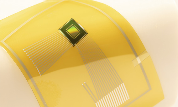
With our many years of experience in the production of CMOS circuits for industrial, research and aerospace applications, we are the ideal partner for the further development of new manufacturing processes and the production of microchips and the processing of wafers. Add-on processes, hybrid flexible foil systems with ultra-thin chips and CMOS-compatible GaN-on-Si processes are further focus of our work.
• Silicon Photonics
• Silicon processing
• Hybrid systems-in-foil
• GaN technology
Silicon photonics
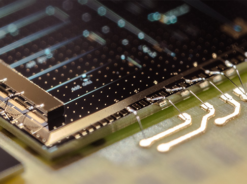
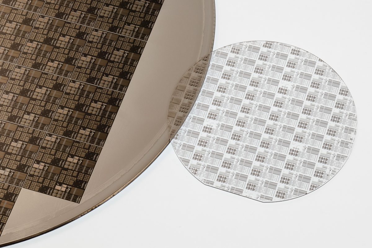
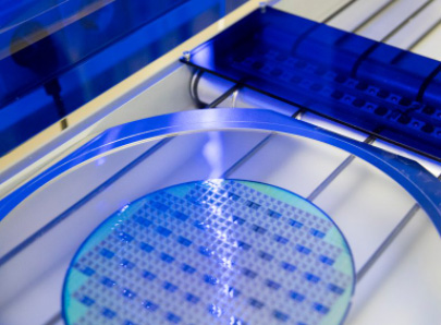
With our new pilot line for silicon photonics, we can manufacture passive and active optical circuits and components, such as on-chip interferometers, ring resonators, active grating couplers, etc. Optical chips are manufactured on 150 mm SOI substrates using CMOS and MEMS technologies. All silicon photonics chips or substrates can be manufactured in-house including the packaging and interconnection technology.
Contact
Mathias Kaschel
email: Mathias Kaschel

We will be happy to support you with our competencies and processes in your projects.
Contact us!
Silicon processing
We look back on more than 30 years of experience in developing various applications and processes in the field of microelectronics and nano technology for both research and industry.
With our modern equipment and a strong network of partners we find solutions for your products and your ideas.
Our range of performance
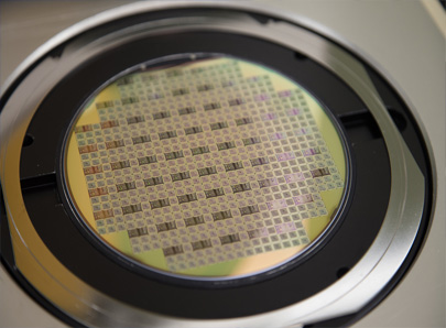
- Qualified individual processes and process chains for silicon and quartz wafers up to 200 mm
- Packaging technology and advanced packaging processes for hybrid foil systems with embedded silicon chips
- IECQ and ISO 9001 certification (process certification in accordance with ISO 90001, manufacturers of microchips according to IECQ)
Our infrastructure
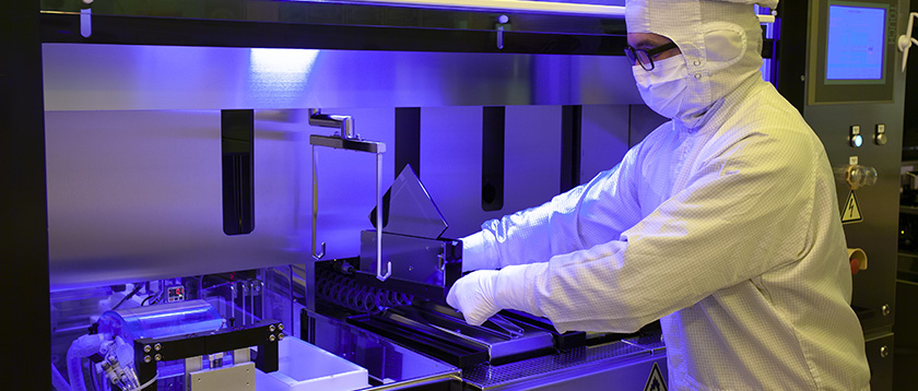
- 1,400 m2 cleanroom ISO 4
- Complete front- and back-end of line process line with Si epitaxy, deposition, metallization and etching equipment
- Mask production line for 6, 9, 12 and 17 inch (450 mm) substrates
- Lithography (i-Line stepper, direct laser writing and direct electron beam writing as well as back and proximity exposure)
- Packaging and interconnection techniques with wafer processing up to 200 mm including backthinning
- Test and quality assurance environment
Hybrid systems-in-foil
Flexible electronic systems with integrated silicon chips are the basis for new products in the fields of medical technology, automation and mobility. Our technologies provide solutions for mechanically bendable and reliable electronics.

Integration of thin chips
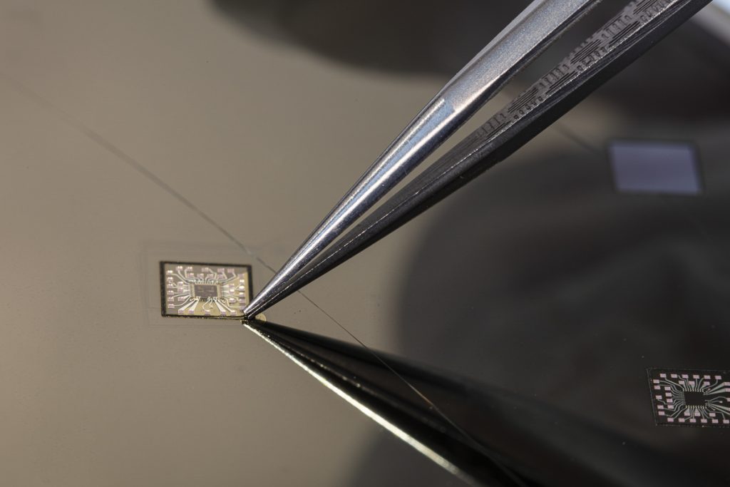
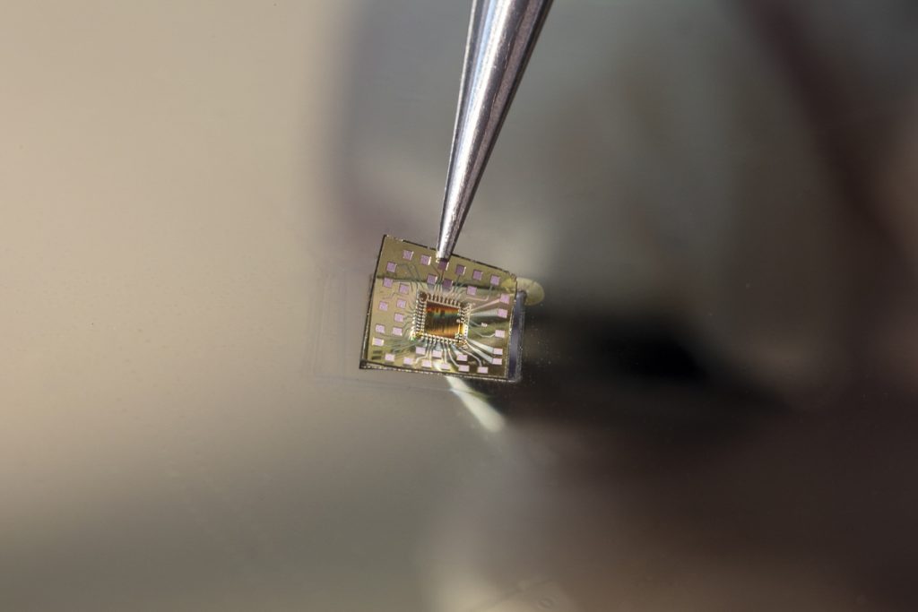
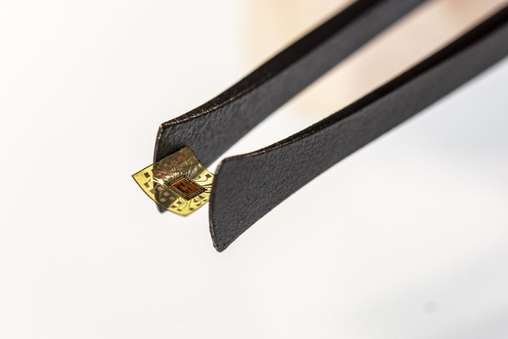
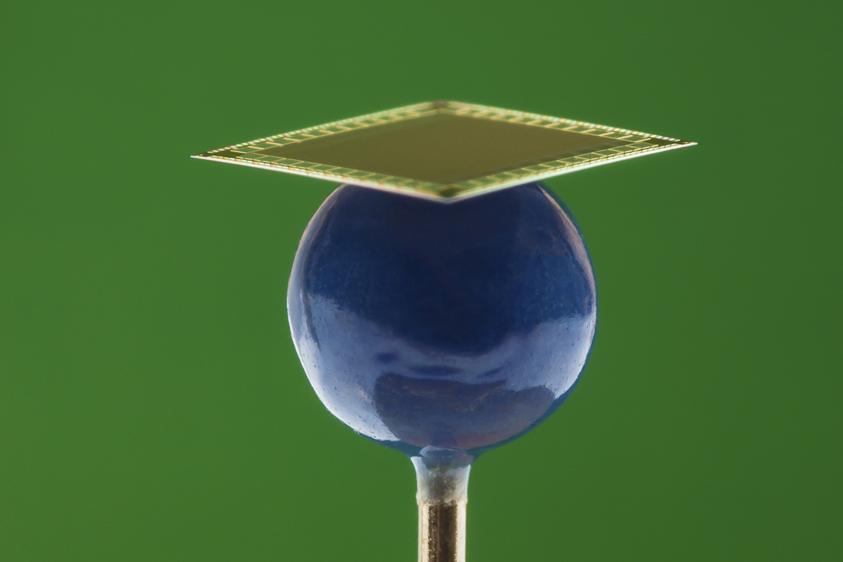
For chip integration, we have techniques to thin wafers and individual dies for thicknesses as thin as 20 µm. We have proven methods to handle and assemble the flexible chips. For chip integration in foil systems, we use the patented Chip-Film Patch (CFP) technology, which allows the contacting of the smallest pad geometries (< 5µm).
Research and Development
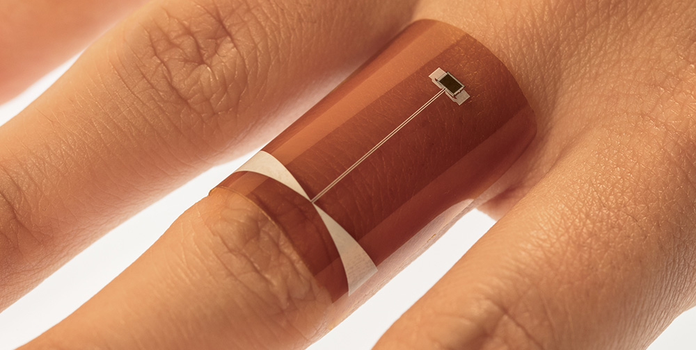
We develop hybrid systems in foil (HySiF) together with partners for various applications. A chip-film patch with evaluation ASIC provides digitization of sensor data for respiratory monitoring of premature infants. Embedded image sensors and communication chips as well as antennas integrated into the foil enable wireless data transmission in the GHz range.
GaN technology
- We process GaN-on-Si wafers in a CMOS-compatible environment. Our range of performance:
- GaN-on-Si technology line for 150 and 200 mm wafers
- Wafers (CMOS-compatible)
- Inline measurement equipment (DC measurements, pulsed and capacitance-voltage measurements on fully or partially processed wafers up to 200 mm diameter)
- Fully automated standard measurements for efficient mapping of essential device parameters for entire wafers
- Customized evaluation software to organize and sort large data sets
