Nano-HySiF – Nano contacts for flexible electronics
Veröffentlicht am

Newsletter 1/2022
New contacting technology for flexible systems
Nano contacts for reliable integration of ultra-thin silicon chips in flexible films

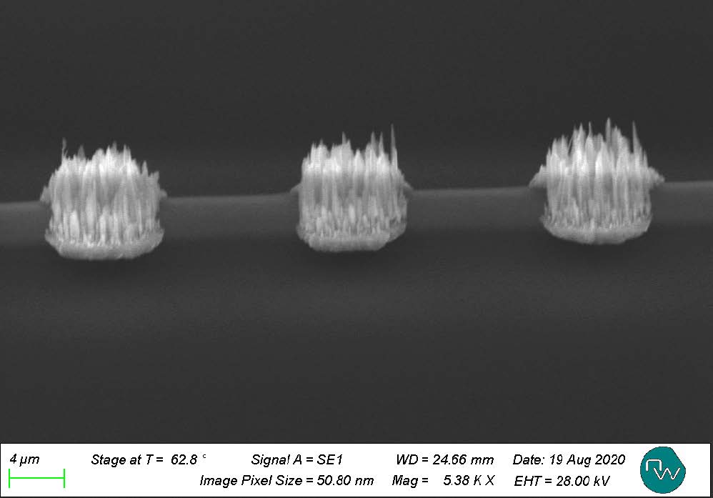
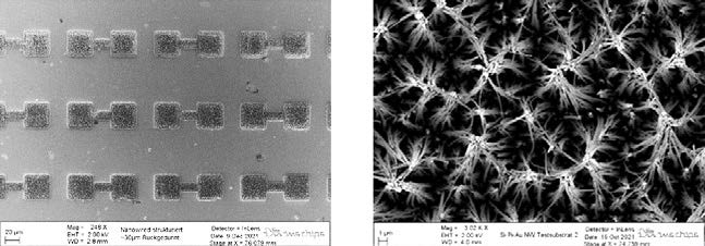
Flexible electronic systems are increasingly conquering market segments, particularly in the fields of medical technology and life style products, while creating a wide range of new products. The development is driven by medical applications, such as catheters, which, when equipped with sensor functions, show significant improvements in work processes and thus in operational safety and patient protection. This is only possible by integrating high-performance silicon components (sensors, ASICs and microprocessors) into the flexible film, because the required functionality cannot be achieved with thin-film components alone. At IMS, these hybrid systems-infilm (HySiF) with embedded thinned silicon chips have been researched for years. Using the patented Chip-Film Patch (CFP) technology, we have been manufacturing flexible multi-chip modules with embedded ASICs and micro controllers in combination with printed sensors and other thin-film components. The wafer-based and CMOScompatible CFP technology facilitates chip interconnections with pad sizes < 10 μm and small pad spacings using adaptive layout processes with laser direct writing. The key factor here is reliable contacting of the various components (sensors, ICs) into the flexible system. The CFP process is similar to semiconductor processes with sputtering and etching processes as well as lithographic structuring. The Nano-HySiF project explores a different approach using nano contacts. Cooperating with the Hessen-based company NanoWired, the IMS has been working on the integration of ultra-thin silicon chips into flexible foil systems since 2021. The hair-thin metal rods can be up to a few micrometers long, depending on the application and contact size. The contact diameters that can be produced with a nano-wiring structure range from 3 μm to several millimeters. The materials of these nano-wiring structures are usually made of copper, but can also be made of gold, silver, nickel or platinum. Once the nano-wiring structures have been created on the substrates, the user has various bonding methods at his disposal, for which NanoWired has introduced the process designations “Velcro-Welding, Velcro-Sintering, Velcro-Glueing”. If there are nano contacts on both workpieces to contact, the joining process can take place at room temperature. Similar to Velcro, the nano structures form mechanical and thus also electrical connections. With modified joining parameters (temperature and pressure), systems can also be joined that have nano structures on only one side of the contact. For chip structures on rigid systems, electrical resistances of < 1 μOhm/mm² and thermal conductivities of 350 W/mK with strengths of up to 60 MPa were achieved. The contacting of thinned and thus bendable silicon chips naturally poses a special challenge to the packaging technology, but offers a variety of advantages for hybrid integration. For example, facedown mounting of chips on the prepared foil simplifies the process considerably, and time-consuming via etching processes on the embedded chips are no longer necessary. With the already proven small contact sizes and pitches < 10 μm and low temperature requirements, the nano-wired technology also enables the direct assembly of small chiplets with minimal structure sizes onto foil systems. When producing medical catheters, minimal dimensions and the size of these chiplets are also crucial. The current project is therefore using a foil with bending sensors for a catheter application to evaluate the technology. Initially, however, the partners will be working with thinned silicon chips that have a variety of different contacts and test structures. Fig. 2 shows such contact pads on these chips

Fig. 2 Scanning electron microscope image of nanostructures on a thinned silicon chip

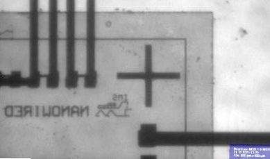
Fig. 3 Infrared image of a joined hybrid foil system with nano contacts.