About us

Institut für Mikroelektronik Stuttgart

Civil law foundation
Member of the Innovationsallianz Baden-Württemberg
Executive Director of the Institute: Prof. Dr. Niels Quack
Foundation: 1983 by the state of Baden-Württemberg
Number of employees: +100
Operating budget: 18,3 million euros

History

2022

Nano-HySiF project
  • IMS CHIPS has initiated, within the Nano-HySiF project, a cooperation with the NanoWired GmbH, which is funded in the ZIM program of the BMWI.
Wafer with AI chips
  • Edge-AI: Joining forces with Hahn-Schickard and FZI, the IMS has developed its own AI chip. The chip contains a RISC-V processor and special AI accelerators and is intended for use directly on sensors.
Springer Theses Prize
  • Dr. Mourad Elsobky has been awarded the Springer Theses Prize for the dissertation done at the IMS.
  • In the HyPerStripes project supported by the Penta program, solutions for flexible interconnects and planar hybrid film systems are being developed.
SensIC project
  • In the SensIC – Flexible Foil Systems for Reliable Electronics project, IMS CHIPS is supporting KIT in a development contract with hybrid foil systems and integration technologies.
PhotonQ project
  • In the BMBF funded PhotonQ project, IMS CHIPS is researching and developing integrated photonic chips with novel components such as extremely low-attenuation phase shifters.

2023


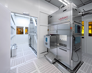
Vistec E-Beam SB255
  • The equipment acquired with REACT-EU funding was put into operation. The investments were used to expand the existing infrastructure at the institute for the large-scale and flexible production and characterization of various nanostructures.

  • The Institut für Mikroelektronik Stuttgart has made significant progress in saving energy. Through a variety of measures, electricity consumption has been reduced by 554,600 kWh, while district heating consumption has been reduced by 467,000 kWh.

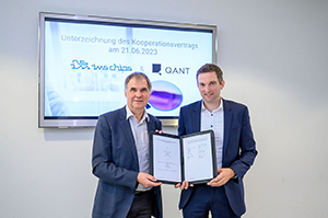
Prof. Dr. Joachim Burghartz and Michael Förtsch, Managing Director of Q.ANT
  • The Stuttgart-based start-up Q.ANT and the IMS have signed an agreement for the joint production of quantum chips. Chips for quantum processors are to be produced in small batches in just two years.
  • The “ALL2GaN” project is about easily integrated energy-saving chips based on gallium nitride (GaN). In the project, IMS CHIPS is working on the further development of existing approaches for the advantageous processing of GaN substrates.

© Kuzmick – stock.adobe
  • SpektroChip – Novel micro-spectrometer system for the near-infrared (NIR) range. The aim of the SpektroChip project is the development, construction and demonstration of a novel micro-spectrometer system for the near-infrared (NIR) range for lab-on-a-chip applications in biomedicine.

2020

  • Deutscher Zukunftspreis 2020 has been awarded to Trumpf and Zeiss as well as to the Fraunhofer Institute for Applied Optics for their project “EUV Lithography – New Light for the Digital Age”. IMS CHIPS supplied high-precision and individually manufactured computer-generated holograms for this purpose, which are used to test and measure the EUV optics.
The Minister of Commerce, Dr. Nicole Hoffmeister-Kraut, delivers the authorization for the “BW CPS” project
  • In the “BW-CPS” project (CPS = cyber-physical systems), an initiative by Hahn-Schickard, FZI and IMS CHIPS funded by the state of Baden-Württemberg, a modular system kit for intelligent and energy-efficient sensor technology for Industry 4.0 was developed successfully.
Multi-Elektrode Chip
  • IMS CHIPS is part of the PanaMEA project funded by the BMBF. The aim is to develop an intelligent implant to measure blood glucose levels. IMS CHIPS is responsible for the development and sample production of the implant´s ASIC.
  • The renowned “Nature” magazine reports on an ultrasonic projector for moving holograms developed at the Max Planck Institute for Intelligent Systems in Stuttgart. This ultrasonic projector is based on a multi-electrode array chip developed and manufactured by IMS CHIPS.
  • IMS CHIPS and Hahn-Schickard are working on a rotary encoder with non-contact scanning in the AiF project INOSENS. The Opto-ASIC required for this is being developed by IMS CHIPS and consists of a large number of integrated photodiodes and mixed-signal circuit elements to determine the angle of rotation position.
Concept for optical particle measurement
  • The ZIM project “Particle Sensor” aims at the development of a miniaturized, fully automated system for the real-time detection and analysis of airborne particles in the form of fine dust and allergy-relevant pollen species in ambient air. IMS CHIPS is developing a silicon photonic chip for this purpose.

2021

MikroSystemTechnik Kongress 2021
  • This year´s MikroSystemTechnik Congress was held in Ludwigsburg. Prof. Dr. Joachim Burghartz acted as chairman of this largest German symposium for microsystems technology.
  • The future cluster QSens from the Stuttgart/Ulm region, in which IMS CHIPS is significantly involved, is one of the winners of the “Clusters4Future” competition. QSens researches innovative quantum sensors that can realize unprecedented sensitivity and spatial resolution.
First Place Best Paper Award
  • For the paper: “Front-End Electronics for Beta-Cell Function Monitoring with an Integrated FOPP Detector”, Dr. Zili Yu and co-authors received the First Place Best Paper Award at IEEE SENSORS.
  • IMS CHIPS was awarded the publication prize of the University of Stuttgart for the publication “Ultra-Efficient Silicon-on-Insulator Grating Couplers With Backside Metal Mirrors”. IMS CHIPS scientists were also involved in the technological development and manufacture for the award-winning publication on integrated optical circuits.
  • The ID2PPAC (Integration of Processes and Modules for the 2-nm Node) project consolidates and integrates the technology solutions for the 2-nm node identified in the previous IT2 project. IMS CHIPS is collaborating in the lithography equipment work package.
  • Im neuen Ausstellungsbereich Mikroelektronik des Heinz Nixdorf MuseumsForums wurden Exponate zur Chip-Herstellung von IMS CHIPS ausgestellt.

2018

Coverstory in IEEE Journal
  • The IMS CHIPS-developed adaptive layout process silicon chips-in-foil systems is the frontpage story of the renowned IEEE journal in its latest May/June 2018 edition..
  • IMS CHIPS is developing customized evaluation ICs to control and analyze the sensor signals as well as integrating its expertise in technologies to embed ultra-thin chips into the foil system in the FLEXMAX project.
ParsiFAl 4.0 project
  • MS CHIPS has joined partners in the BMBF-sponsored research project ParsiFAl 4.0 on the development of new sensors and electronics on thin foil for Industrie 4.0
  • IMS CHIPS has developed ultra-precise diffractive optical elements (DOEs) for surface monitoring of EUV mirrors and researched concepts for mask architecture as part of the ECSEL/BMBF project SeNaTe. This continues in the follow-up projects TAKEMI5 and TAPES3.
  • The POSITION-II project´s objective are innovative ideas for intelligent catheters and implants by introducing open technology platforms. The IMS is responsible for the development and operation of ASICs in the sub-project “digitaler MRT-sicherer EP Katheter”.
  • The aim of the BMBF-project “OPALID” is the research and development of a small, reliable and cost-efficient LiDAR system. The IMS is responsible for the system´s sending unit on a silicon photonic chip.

2019

EUV stepper system with sketched beam path of the EUV light
  • Within the ECSEL/BMBF project TAKEMI5, IMS CHIPS researched mask infrastructure and new concepts for mask architecture.
Wafer with Si energy filter membranes
  • The ZIM-funded joint project with the start-up company mi2-factory for the development of a large-area energy filter membrane for single-wafer ion implantation in silicon carbide was successfully completed.
  • The innBW Implant project – Chip-in-foil systems for bio-electronic medicine – has successfully been completed.
Fully automated standard measurements of high-performance electronics
  • The MOCVD 4.2 project is to develop an increase the production capability of the MOCVD (Metal Organic Chemical Vapour Deposition) technology for applications in power electronics, in photo voltaic as well as in nano photonics and sensor technology.
  • In the joint project NeMoH – Neuromorphic Hardware – coordinated by IMS CHIPS, together with the Research Center for Information Technology (FZI) and the Hahn-Schickhard-Gesellschaft für angewandte Forschung e. V. (HSG) to develop microelectronics for artificial intelligence.
Dürr Supplier Award ceremony
  • IMS CHIPS receives the Dürr Supplier Award 2019 in the Innovation & Technology category for innovative product solutions. Dürr and IMS CHIPS are continuously researching future technologies.

2016

Lithium-ion cells with embedded system to monitor functions
  • The Smart-LiB project is designed to research solutions to encompass the Li ion battery staple´s condition without the currently required wiring.
Photonic chip with echelle grating for fast optical data communication
  • On June 23rd, IMS CHIPS successfully held its first photonics workshop. It offered an outlook on various subjects and applications in photonics..
  • As part of the BMBF project NEMEZU, new, precious metal-free membrane electrode units for alkaline fuel cells of the future are being researched and developed.
  • IMS CHIPS was awarded as one of “100 Orte für Industrie 4.0 in Baden-Württemberg”.
Minister of Economic Affairs Dr. Nicole Hoffmeister-Kraut handed over a funding notification
  • IMS CHIPS has been supporting industrial companies in Baden-Württemberg and beyond for over 30 years. This was commemorated by a celebration organized by the IMS Scientific Association with Minister of Commerce, Dr. Nicole Hoffmeister-Kraut, as special guest.

2017

  • The IMS has received a 3 million Euros sponsoring by the Ministry for Economics to aid the switch of its research infrastructure to the 22 mm wafer technology.
TENECOR EEG chip
  • The BMBF project TENECOR (telemetric multi-module neonatal cortex monitoring) to determine tiny biomedical signals has been completed successfully.
  • Muhammad Alshahed has been awarded this year´s best “Young Scientist” Paper Award at ESSDERC.
  • As part of the sponsoring program “Photonik Forschung Deutschland” the BMBF project MULTI-3D will be developing a micro-optical 3D sensor system to determine and/or measure 3D objects.
6” GaN on silicon and 2” bulk GaN wafer
  • Two GaN technology projects have been launched at the IMS. The DFG project C-GaN – Complementary GaN for High Temperature Electronics and the KMU-innovativ project GaNScan – Mapping and Modeling of GaN/Si-Wafers for Power Electronics Applications.
innBW institute
  • Review: innBW research facilities´ performance excellent This conclusion was drawn by the high-ranking reviewer panel which had been scrutinizing the non-university research facilities on account of the Baden-Württemberg government in recent months.

2014

FlexPacFAM – flexible packaging
  • The FlexPacFAM project – flexible packaging of micro system components based on circuit board carriers using Film Assisted Molding has been successfully wrapped up.
Photo diode ASIC placed on laser diode
  • The X-MIND project researching extremely miniaturized optical speed sensors has been launched.
Intelligent Service Robotic through 3D imaging and processing
  • INSERO3D „Intelligent Service Robotic through 3D imaging and processing” is an integration platform SSI (Smart System Integration) project. Technological solutions for the intelligent optical positioning of service robots in a selected area and/or for an interactive object have been realized.
Self-adapting intelligent multi-aperture camera module
  • IMS CHIPS is participating in SITARA. The project´s focus is the development of more cost-effective, intelligent and high-light cameras with a high-dynamic range and very short face-to-face dimensions of less than 3mm.
Granting of the J. J. Ebers Award
  • Prof. Joachim N. Burghartz receives IEEE Electron Devices Society´s J. J. Ebers Award 2014 Joachim Burghartz received this internationally renowned top honor during the microelectronic expert conference IEDM on December 15th.

2015

VPG400 laser direct writer from Heidelberg Instruments
  • A one-day colloquium was held after the laser direct writer, which was procured with ERDF funding, was put into operation. The laser direct writer can be used to create maskless micro structures on various substrates
Foil-based silicon needles
  • The “Intelligent Implants” research project includes foil implants that are as small and flexible as possible. This platform development opens up entirely new paths for the treatment of diabetes and for the diagnosis, therapy and rehabilitation of brain diseases.
MEMS – DMFC fuel cell
  • MEMS – DMFC (direct methanol fuel cell based on micro electric mechanical systems) project launch The aim of the project is to develop MEMS cells based on silicon semiconductor technology.
Loading the etcher with a DOE blank
  • SeNaTe – Seven Nanometer Technology – project launch. Ultra-accurate Diffractive Optical Elements (DOE) for a surface inspection of EUV mirrors are developed and new concepts for mask architecture are explored. The ECSEL project is accompanied by a parallel-running BMBF project.
Finalizing MicroTEC Südwest Spitzencluster
  • On October 26, the central results of the 5-year MicroTEC Südwest Spitzencluster funded by the BMBF were presented. The IMS was significantly involved here via the production platform PRONTO.

2012

CATRENE Innovation Award
  • The EXEPT BMBF sponsored joint project that researches new technologies for the chip production was awarded the Innovation Award 2012 as most innovative project during the European Nanoelectronics Forum München.
  • The third Microsystem Packaging Workshop (PackMEMS 2012) was held at the Institut für Mikroelektronik Stuttgart. The event focused on important trends in packaging technologies.
Demonstration Award
  • Equally successful wrap of the BMBF joint venture HiDRaLoN. The project was awarded the Demonstration Award during the European Nanoelectronics Forum 2012.
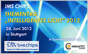
  • Thementag “Intelligentes Licht” at the IMS. Key players from the scientific and industrial world shared information and discussed the future solid-state light sources: LED and OLED.
  • This year´s successful “Beams and More” workshop at the IMS commemorated its 10th anniversary. The “Beams and More” workshop has established itself as a constant since it was launched in 2003.

2013

KoSiF “complex systems in foil”
  • The BMBF-sponsored KoSiF project has been launched – industry and science teaming up on bendable and autonomous sensor systems.
  • The IEEE Spectrum has published a feature article titled “Make Way for Flexible Silicon Chips” on the IMS Chipfilm™ technology in its March issue.
Opening ceremony of the clean room expansion
  • Opening ceremony of the clean room expansion at the Institut für Mikroelektronik Stuttgart Baden-Württemberg´s Minister of Finance and Economy, Dr. Nils Schmid, and Stuttgart´s mayor, Fritz Kuhn, to inaugurate the new clean room.
Photonic integration
  • Together with the Institute of Electrical and Optical Communications Engineering (INT) of the Universität Stuttgart the IMS reached a world record in energy-efficient photonic integration in silicon.
IEEE EDS PhD Fellowship Award 2013
  • Tarke Zaki has been awarded the IEEE EDS PhD Fellowship Award 2013.

20009

Gaussian Shape Beam by NIL Techno
  • A new cooperation in the nanoimprint lithography field. The leading manufacturer for dies in nanoimprint lithography,NIL Technology, and IMS CHIPS announced the start of their cooperation in the nanoimprint template field during the NILCOM meeting.
Jack Raper Award
  • IMS is awarded the “Jack Raper Award” in San Francisco. The “Jack Raper Award for Outstanding Technology Directions Paper” was awarded for the presentation “CMOS Imager Technologies for Biomedical Applications”.
Hyperbraille Display
  • Within the “Hyperbraille” project the IMS, METEC AG and several other industrial partners develop the 2D braille script display enabling the vision-impaired an interactive access to graphic user interfaces.

2010

REM image of an electron beam deflection unit for the “CHARPAN” project
  • As to nano structuring for future chip generations the IMS is significantly involved in the international “CHARPAN”, “FANTASTIC” and “MAGIC” projects.
  • The Landesforschungspreis für Angewandte Forschung was awarded to Professor Dr.-Ing. Joachim Burghartz in a ceremonial act in Stuttgart.
  • IMS CHIPS is awarded Spitzencluster MicroTEC Südwest
TanDEM-X – radar satellite
  • Mounted on the TanDEM-X radar satellite another satellite is leaving the Baikonur space port into space equipped with special ASICs.

2011

Cleanroom ground breaking ceremony
  • The ground-breaking ceremony for the clean room construction took place on the institute´s premises in Stuttgart on February, 15th.
innBW Innovation Alliance Baden-Württemberg
  • The Institut für Mikroelektronik Stuttgart together with 11 other research facilities in Baden-Württemberg forms the Innovationallianz Baden-Württemberg.
  • The non-profit association of sponsors Förderverein des Instituts für Mikroelektronik Stuttgart founded in 1983 has been restructured into Forschungsverein and expanded its range of services.
First PRONTO workshop
  • More than 80 participants from industry and research gathered for the PRONTO workshop in Stuttgart.
GMM-Preis 2011
  • GMM prize 2011 awarded to the IMS for the IEDM paper “Ultra-Thin IChip Technology for System-in-Foil-Applications”.
 

2007


SafetyEYE® camera system
  • The IMS delivers HDRC® image sensors specially developed together with DaimerlChrysler for the Pilz SafetyEYE® camera system.
  • The IMS developed and manufactures Retina chip is the first chip in the world tested on blind patients giving them simple seeing impressions.

REM image of a template with 60 nm pillars for the “FANTASTIC” project
  • IMS develops die for the nanoimprint technology and establishes partnership to the MEDEA “FANTASTIC” project.
  • GATE FOREST® will be enlarged for Structured ASICs using a 0.5 µm process

Ultra-thin microchip: 20 µm thickness
  • IMS and Bosch enter into a cooperation agreement for the development and application of technologies for ultra-thin microchips.
  • IMS presents a camera measuring temperature using quotient pyrometry.

2008


Webseite VIP
  • In cooperation with the Fraunhofer Institutes IAO und IAT and several small and medium-size companies the IMS develops the innovation guideline “VIP – Von der Idee zum Produkt”.

Radar satellite TerraSAR-X
  • The TerraSAR-X satellite made by the satellite manufacturer Astrium takes off into space successfully.
    On board there are numerous space-qualified IMS ASICs.

IdeenPark 2008 in Stuttgart
  • The “IdeenPark” attracts more than 300,000 enthusiastic visitors.
    The IMS is represented with lectures and a well-frequented booth in the SchlauLoPolis area.

Festive ceremony at Haus der Wirtschaft in Stuttgart
  • The Institut für Mikroelektronik Stuttgart commemorates its 25th anniversary.

Ultra-thin RFID chip on foil substrate
  • In order to research a new generation of high-dynamic, high-resolution and low-noise image sensors the comprehensive project cooperative HiDRaLoN (High Dynamic Range Low Noise CMOS Imagers) has been established within the European research project CATRENE.
  • In order to research a new generation of high-dynamic, high-resolution and low-noise image sensors the comprehensive project cooperative HiDRaLoN (High Dynamic Range Low Noise CMOS Imagers) has been established within the European research project CATRENE.

2004

Cantilever Array
  • Wafers with MEMS structures are successfully manufactured at the IMS. The young CavendishKinetics company partners with researchers at the IMS to develop silicon nano relais for future non-volatile storage units.
  • Within the “XTUMASK” and “Second Level Imaging” projects technologies for the manufacture of masks with future technology notes are developed and equipment and materials are evaluated.

2005

EUV full field masks
  • IMS manufacture of the first EUV full field masks with minimal structures around 100 nm for ASML.
  • Together with the Lange Feinwerktechnik and Staiger companies the IMS develops extremely compact pneumatic valve unit with integrated control electronics. Work pieces within the sub-millimeter size can thus be handled with a clock cycle of below 20 ms – an important precondition for the rational manufacture of tiny precision components.
Joachim Burghartz
  • As of October 1st, 2005, Prof. Dr. Joachim Burghartz is Chairman of the Board of the IMS and Full Professor at University of Stuttgart. He succeeds Professor Dr. Bernd Höfflinger who has retired.
Image sensor chip IVP
  • Manufacture of miniaturized image sensor chip IVP for use in swallowable video pill and integrated into an endoscope.
  • After finishing animal testing the sub-retinal implant using an IMS chip is implanted into humans for the first time.

2006

  • As part of the EU project CHARPAN the IMS participates in the development of a multi-ionbeam pattern generator.
Chipfilm
  • The IMS demonstrates a new process to fabricate extremely thin chips in cooperation with the Institut für Physikalische Elektronik (IPE) of Universität Stuttgart and presents this during the renowned International Electron Devices Meeting (IEDM) in San Francisco.
  • The IMS paper is awarded Best Paper Award during the Photomask Japan 2006 conference.

2001

IC_Lab experimental board
  • IC_Lab – the experimental board to design complex digital electronics. Practical exercises from the FeLS and IC lab can easily be realized on the experimental board.
Klaus von Klitzing
  • The practical lab course “Schülerinnen und Schüler machen Chips” commemorates its 10th anniversary. Nobel prize winner Klaus von Klitzing of the neighboring Max-Planck-Institut für Festkörperphysik in Stuttgart inspires young listeners during the ceremony.
ZBA350
  • Installation of the ZBA350 Leica e-beam direct writer at the IMS.
  • Mixed-signal ASIC manufactured for the new high-resolution and high-dynamic absolute-value transducer generation “Dignalizer” made by Baumer Electric AG.

2002

APS star sensor camera
  • Star sensors determine the position of satellites and space probes by using patterns of star constellations. The IMS develops a radiation-resistant image sensor for long-term emissions in cooperation with the Institut für Physikalische Elektronik (IPE) of Universität Stuttgart.
  • Within the “TranSi” project, the IMS jointly develops transferrable thin Si layers und tests their application during the production of CMOS circuits with the Institut für Physikalische Elektronik (IPE) of University of Stuttgart.
  • Installation of a modern line of masks at the IMS.
  • ASIC no. 1,000,000,000 is manufactured at the IMS.
  • Founding of IMS VISION GmbH as Joint Venture with OMRON
10000 pixel – line sensor
  • HDRC® line sensor The IMS develops a high-resolution image sensor with a 10 cm image line for space applications.

2003

  • Within the framework of the ABBILD project the IMS participates in the development of selected areas of mask technology.
Photomask Best Paper Award
  • During the Photomask Conference in Monterey, USA, the IMS is awarded the BACUS Poster Award for the presentation of the “phase shifting masks within the 65 nm technology node”.
  • The IMS mainly develops and manufactures numerous optical components for the Zeiss SMT AG company for the test engineering area.
HIPSCAN System
  • The IMS is partner to the “HIPSCAN” EU project predominately concentrating on high-speed scanning of paper documents. A cryto ASIC is developed at the IMS enabling the realtime encryption at extremely high data rates.

1998


MORE-Phone
  • Under guidance by the IMS the EU project “Mobile Rescue Telephone” develops the first mobile phone worldwide with an integrated GPS positioning module.
    The central core of the phone is an IMS GATE FOREST® ASIC.

Aircraft docking system
  • The weatherproof HDRC® camera aircraft docking system by GEVITEC and Honeywell Airport Systems is installed at the gates of international airports, such as airports in Barcelona, Billund, Brussels, Dresden, Hanover, Leipzig, Madrid, Beijing, Canton, Seoul and Tel Aviv.
    The video-based guided docking system guides the pilot through a display mounted at the airport facility when approaching the gate and enables an exact parking position in order to dock on the gangway.


SIOP SIOP neuro processor chip
  • Based on the SIOP neuro processor the SAND neuro processor was developed that is integrated into the NNSIM neuronal network simulator, a powerful platform for neuronal applications developed at the IMS.

1999


Retina implant
  • The IMS, the NMI in Reutlingen and the Klinik für Augenheilkunde Tübingen jointly present the idea of a retina implant during the Hanover Fair.


SOI membrane mask
  • The IMS is partner to the “100 nm mask writer” and supports the equipment development with the relevant process development.


Recording using HDRC® camera
  • First color images recorded with HDRC® cameras


FeLS start screen
  • The FeLS learning tool (FPGA design – a autodidactic learning tool) is developed. It teaches the theoretical fundamentals of digital technology and its applications as well as the simulation of circuits all the way to the FPGA download.

2000


Low-Power Design Award
  • The IMS is awarded the “Low Power Design Contest” at the IEEE Computer Elements Workshop in Arizona.

  • Web-based “TEAM 2000” learning system for engineers and circuit developers is introduced.


T-Gate (REM image)
  • CMOS process HIPERLOGIC transistors developed at the IMS with 100 nm structures working at an operating voltage of 0.5 V are presented.


Circular line sensor
  • Manufacture of circular line sensors with 2048 pixels on its circumference.

  • Radification of a HDRC® licensing and development agreement with SHARP.

1995


Single chip controller
  • Within the “Mikrocontroller-Baukasten” project the Intellectual Property (IP) library with functional modules for ASICs, such as the field bus module, processing cores and A/D converters are created.
    Several small and medium-sized companies have joint the ASIC Working Group at the IMS and use the IP Pool for their ASIC developments.


CECC EN 100114 part 1 certification
  • The IMS is certified as chip manufacturer in accordance with CECC EN 100114 part 1.
    The IMS is awarded the certificate, proving the high quality standards in development and manufacture of ASICs made at the IMS.
    CECC EN 100114 part 6 certification.


EDA award
  • The tiniest 5 kW pulse converter in the world:
    Novodrive ND 21.
    This remarkably tiny tool was made possible by the ASIC-NOVOCHIP that was developed jointly by NOVOTRON and the IMS.
    Awarded the EDA Award for “best ASIC_Design”.

  • The PROMETHEUS project, a European EUREKA initiative is completed.


1996

  • As part of the “Electronic Eye" project DB and the IMS develop an image processing system based on serially transportable analog image data with a neuronal link.


VISION prize 1996
  • 1st prize awarded to the HDRC® image sensor for the field of applied image processing during the VISION trade fair 1996.


EASIE model trial
  • As pilot project the EASIE project is initiated through a cooperation between the BIBB and the industrial trade learning centers (ETZ, EAZ) and industry (BBT) by integrating modern microelectronics into the vocational training of electrical trades.

  • Production of 0.8 µm GATE FOREST® ASICs


1997


Loglux camera
  • Initiation of Loglux as first HDRC® serial product.


1. Photo diode array for subretinal implants
  • The IMS develops the first photo diode arrays to be used for future sub-retinal implants of the vision impaired.

  • In cooperation with Bosch the IMS develops a special camera for “Robust Vehicle Vision” to use in image processing systems for vehicles.
    The 0.35 µm IBM technology HDRC-type image sensor has 720 x 576 pixels with a 13.5 µm pixel distance, integrated AD and DA converters and special circuits to support wafer tests.

  • Development of the Si membrane technology.

  • A license and development contract for HDRC® sensors with VGA resolution is concluded with G-Link (USA, Taiwan).

1992

SMC group picture

  • The first “Schülerinnen und Schüler machen Chips” (SMC – practical course for students) is held at the IMS.


Basic patent HDRC®-Bildsensoren
  • The IMS patents the basic patent for highly-dynamic HDRC® image sensors.

1993


3D Chip
  • Comprehensive and successful research is carried out at the IMS regarding the 3D integration of CMOS circuits.
    The results of chips with “piled-up transistors” draw attention among the experts.


ISO 9001 certification
  • The IMS is being awarded the ISO 9001 certificate.

  • Within the framework of the PRO CHIP project, the first image sensor with 64 x 64 pixels in accordance with the patented IMS HDRC® principle is presented.

  • Joint evaluation of the ZBA31H e-beam writer with Jenoptik at the IMS.


1994


Bosch radio equipment with IMS HF transistors
  • Development and serial production of HF power transistor stages in bipolar technology for Bosch radio equipment within VHF and/or UHF transmission of up to 480 MHz with 7 Watts power.


Vector Arithmetic Coprocessor
  • Together with researchers from the Karlsruhe Research Center for Information Technology (FZI) a complex “Vector Arithmetics Coprocessor” is developed and manufactured at the IMS.


SAND Board
  • The neuro processors department develops SIOP, a digital neuro-processor enabling realtime neuronal applications, in cooperation with GEMAC mbH.

1989

2-µm-GATE FOREST

  • The IMS GATE FOREST® production is switched over to the 2 µm process with double layer plating

  • The simulator for neuronal networks NNSIM is developed.

  • Development of the QBP chips (Quadrupel Broadband Port) for SEL-Alcatel on the IMS largest GATE FOREST® master.


1990

COMETT course participants

  • The IMS produces the educational COMETT (Community Action Program for Education and Training for Technology in the European Community) video seminars, the most important multilateral EU program sponsoring the cooperation between universities and industry.

Test structure layout

  • Within the framework of the JESSI Project AC41 “Technology Assessment” testing structures, measurement and evaluation processes for the then up-to-date Deep Submicron technologies were developed in cooperation with Alcatel-SEL, Siemens, STMicroelectronics, Bosch among other companies and standardized within the scope of CENELEC.

MCM on Si carrier

  • IBM joins the IMS in the development of a technology for MCMs on Si carriers. The carriers connect 9 VLSI chips into a high-power CPU replacing the multilayer ceramics.

1991

AMK ASIC „AC3“

  • The Arnold Müller Kirchheim (AMK) company mandates the IMS with the improvement and advancement of an American chip manufacturer´s ASIC.
    The “AC3” GATE FOREST® ASIC develops into a AMK key component of the pioneering fully digital drive and control system “AMKASYN” for electrical engines in industrial equipment.
    The “AC3” is still produced today.

Wafer bonding

  • The IMS develops the wafer bonding process and uses it successfully.
    Besides fundamental research regarding bonding and characterization Silicon-on-Insulator (SOI) wafers were manufactured for automotive applications.
    A power component developed with this technology was integrated into IMS-made SOI wafers together with CMOS circuits.

6 inch wafer

  • The IMS technology is switched from 4 inch into 6 inch wafers, GATE FOREST® is produced using a 1.2 µm process.

1986

Inauguration ceremony

  • Completion of clean room and operational startup of semiconductor production line at the IMS.
    In a ceremony the Baden-Württemberg prime minister at the time, Lothar Späth, formerly inaugurated the institute.

Clean room

  • Die ACMOS-Technologie von Siemens wird am IMS eingeführt.

1987

Hohner chip

  • The Trossingen-based Hohner company mandates Intermetall in Freiburg with the volume production of the “Hohner chips” developed by the IMS.

  • The first CMOS microchips are manufactured using a 3 µm process.

  • The IMS Association of Sponsors donates 1 million German marks to the IMS that is then used to set up a quality and reliability laboratory.


1988

HL700 e-beam writer

  • Operational startup of the HL700 electron beam direct writer.

Control chip for fluorescent displays

  • The IMS implements the so-called “SME program”.
    Among others an integrated display driver chip to control fluorescent displays of weighing scales developed by the Bizerba company in Balingen is designed.

„Multi-Projekt-Chip“

  • The Heilbronn University holds the first Workshop of the Multi-Projekt-Chip (MPC)-Gruppe.
    It enables cost-efficient access to the manufacture of microchips for universities.
    The topic of the opening discussion of the workshop is the foundry service at the IMS open to all MPC members.
    In the years to follow the IMS continues to develop numerous chips for the MPC group.

1983

Prof. Ernst Lüder
  • Entry into the Stuttgart foundation registry as “Institut für Mikroelektronik Stuttgart” on July 18th, 1983.
    Prof. Ernst Lüder becomes founding director of the institute.

  • The non-profit Verein der Förderer für Mikroelektronik in Stuttgart e.V. (IMS Association of Sponsors) is founded.


1984

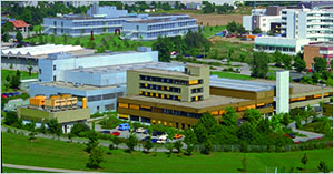
IMS CHIPS Gebäude 1992

IMS facility

  • At the newly established IMS plans for a clean room with a modern semiconductor production line, computer-based design tools and a testing lab for microchips are in full swing.

1985

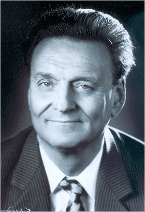
Prof. Dr. Bernd Höfflinger

Prof. Dr. Bernd Höfflinger

  • In record time between spring and fall the clean room buil­ding is erected and put into operation. There are 700 square meters available in the clean room and twice as much space for clean room technology, labs, offices and the shop for work on microchips.

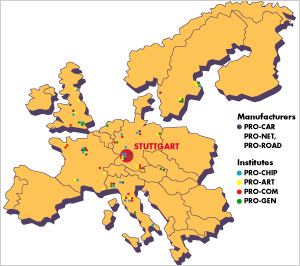
Projekt PROMETHEUS

  • Within the scope of the European initiative EUREKA the PROMETHEUS project is born. It consists of a cooperation between the IMS, Bosch, Daimler-Benz, Siemens and VW and outlines the basics for modern safety features in vehicles: ve­hicle interval radar, surface recognition, track assistance.
  • Acquisition of an electron beam writer has been applied for.