ALL2GaN project
Veröffentlicht am

Patented IMS nanohole technology in the ALL2GaN project
Threshold-Voltage-Engineered GaN HEMTs for high frequency, power and MEMS integrated circuits

Last year, the European ALL2GaN project was launched in response to the European Chip Act and the challenges of climate change. The aim is to bring together European players in the field of power and high-frequency electronics to create a common ecosystem in which energy-efficient GaN ICs can be manufactured on an industrial scale.
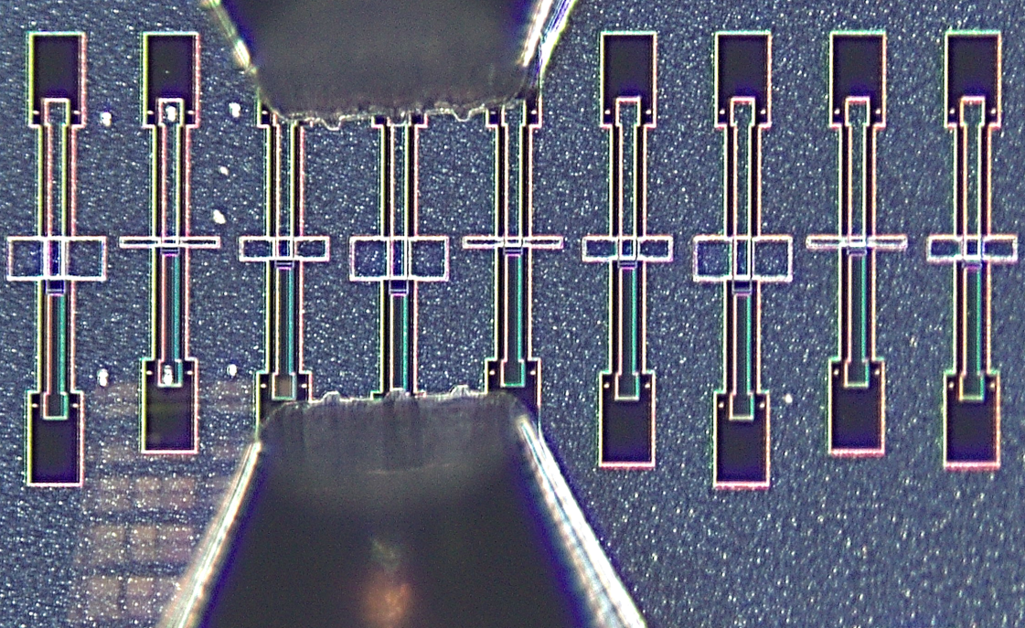
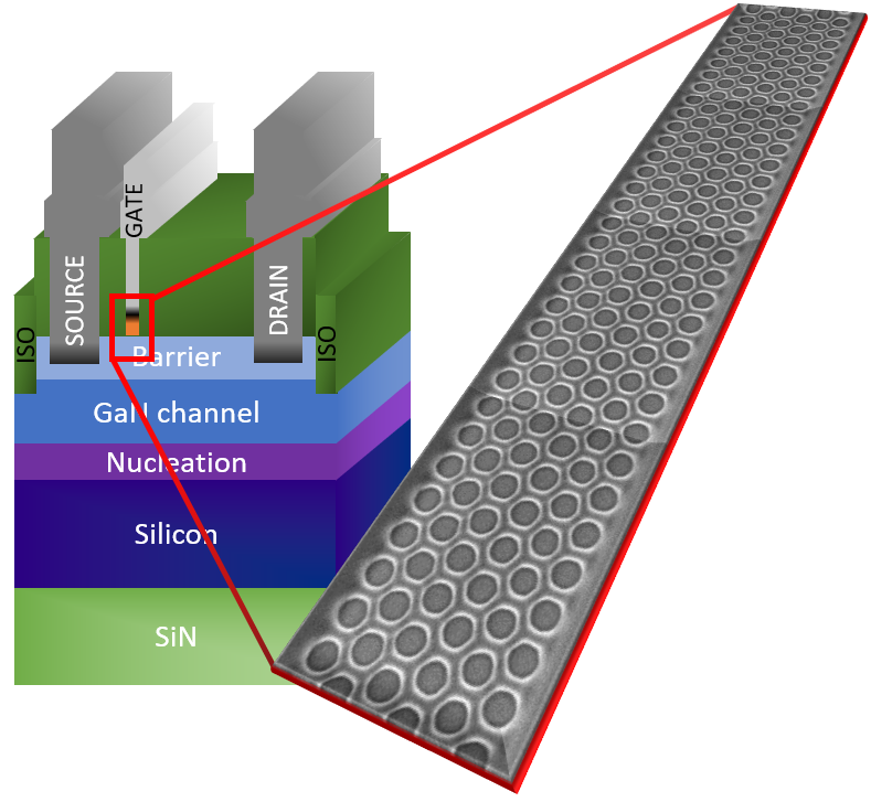
Among the 45 partners from all over Europe is the IMS, which will be working on the further development of the patented nanohole technology on GaN-on-Si wafers as part of the project. This technology is a method to structure the gate areas in GaN HEMTs by means of which the switch-on voltage of the transistors can be changed in a targeted manner. This enables the simultaneous production of GaN transistors with specifically adjusted switch-on voltage within thesame IC.
The idea is to produce transistors for a wide range of applications on a single wafer using the same technology, which can include high-frequency, power and MEMS components.
Following the successful demonstration of the technology, the work within the ALL2GaN project represents the next development step towards Threshold-Voltage-Engineered HEMT ICs.
In cooperation with SweGaN (Linköping, Sweden), the portfolio of the IMS GaN process is also being expanded to include the processing of GaN-on-SiC wafers, which are manufactured using QuanFINE technology. The circuits produced in this work package are primarily used for process development and material characterization on this new type of material system and complement the existing component production on GaN-on-Si wafers.
Contact: Matthias Moser • phone +49 711 21855-479 • moser@ims-chips.de