Automated optical throughput tester for integratedphotonics
Veröffentlicht am

Newsletter 1/2023
Automated optical throughput tester
800 to 1000 measurements per hour with high reproducibility

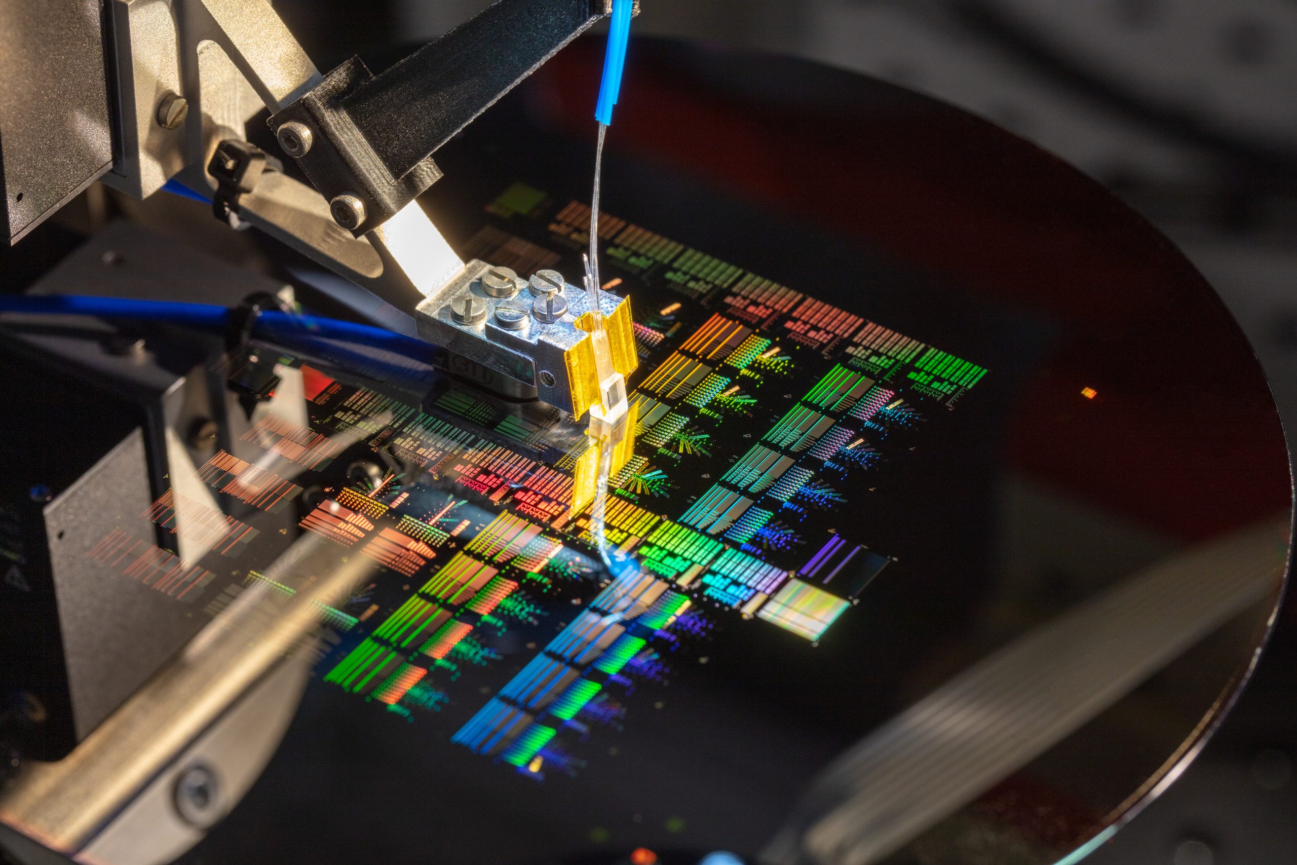
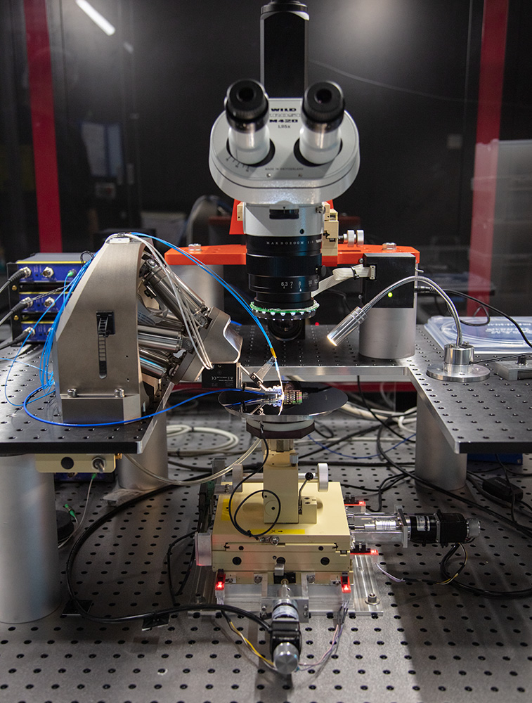
A new optical measurement setup for the characterization of integrated optical circuits has been commissioned at IMS. Its main purposes are the final inspection of photonic chips, characterization of new processes in the silicon photonics line, and qualification of the design of new or improved photonic devices. Fast and reliable optical measurement technology is essential for this. Extensive design parameter variations as well as the reliable extraction of various performance quantities often require characterizing hundreds or thousands of test circuits. For this reason, a new partially automated optical prober was developed from a manually operated semiconductor prober equipped with a hexapod and a piezo positioner. A new software framework was implemented, a capacitive distance sensor was integrated, and the optical signal paths were optimized. Above all, it is the high mechanical precision that now enables throughput spectra to be recorded with a reproducibility of ±0.25 dB.
The setup can be used to measure integrated photonic circuits on single chips up to 150 mm wafers in the wavelength range of 1510 – 1610 nm. Grating couplers within an area of about 10 x 10 mm² are automatically addressed one after the other at a speed of 800 to 1000 throughput spectra per hour. Areas of a wafer beyond this can be reached by simply moving the wafer stage, which currently still requires a new manual alignment. A quadruple fiber array is used to couple and decouple the light, of which one fiber is used to inject light into a coupler, and three fibers are used to simultaneously measure output powers.
Currently, the optical measurement setup is being further upgraded so that a real-time adjustment of the polarization as well as a wavelength range of 1450 – 1650 nm will be available in the future. Other upgrades planned for this year include the integration of current and voltage sources to measure active electro-optical components, as well as an automated wafer stage to achieve full automation.
Contact
Kevin Edelmann
Phone: +49 711 21855 253
e-mail